AI’s on-screen iterations, including the use of generative AI in chatbots, have been grabbing the majority of the world’s attention since the debut of ChatGPT in late 2022. For its next act, AI will move out of the cloud to devices at the edge − with the future of AI being off-screen and in the physical world.
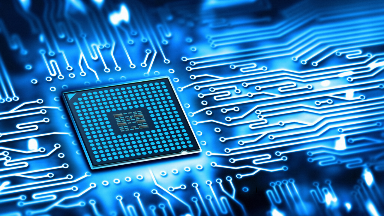
This move will supercharge robotics and IoT, and the technology driving it all will be compound semiconductors, including the material gallium nitride (GaN). Compound semiconductors, or computer chips made from two or more elements as opposed to single-element silicon, are becoming increasingly important in areas where higher performance is required.
AI’s future at the edge cannot happen without compound semiconductor materials that outperform silicon in three key ways. First, they operate very efficiently at RF frequencies. Second, they are effective emitters and detectors of light over a broad spectrum. Third, they are very efficient, particularly in harsh environments for such things as power conversion.
Increased functionality of devices at the edge
The transition of AI off-screen into the realm of IoT means that the devices at the edge will need to get more capable. For example, they will be required to ‘sense’ their environment in ultra-high resolution − meaning that 3D recognition and LiDAR systems like those employed in mobile handsets will become essential for all sorts of devices where this capability is not needed today.
This is a realm pioneered by compound semiconductor lasers and detectors that employ gallium arsenide (GaAs) and indium phosphide (InP), and improved versions of these devices will be necessary for AI progression. Furthermore, it is not only physically sensing things in three dimensions that will be important; wearable health monitors use compound semiconductor materials for biological sensing, an area poised to be revolutionized by off-screen AI.
Finally, the next version of AI will require ultra-fast, ultra-reliable, low latency connectivity even with things at the edge, and the excellent RF properties of compound semiconductors, particularly GaAs and GaN, will be exploited to enable this capability.
Increasing efficiency, reducing power demands
When it comes to AI, much of the world’s attention is currently focused on the energy needs of data centers, and rightly so – and if all data centers around the world were converted from silicon to GaN by the end of the decade, it is estimated that energy loss would be reduced by 30% to 40%. To put that into perspective, the conversion would save more than 100 terawatt hours and avoid 125 megatons of carbon dioxide emissions.
While much of the compute is expected to move to the edge for the next iteration of AI, the energy requirements will remain high; energy usage will scale regardless of whether the compute is occurring in the cloud or at the edge. This makes compound semiconductor materials a necessity for AI to progress.
In addition, the compound semiconductor material GaN is very robust, making it ideal for edge devices such as robotics that operate in harsh environments with elevated temperatures, higher humidities, and the like.
It is easy to see how this will benefit industrial robotics at the edge, but GaN’s capability could take things further, even as far as outer space. MIT researchers recently demonstrated that GaN was able to tolerate exposure to more than 900°F for 48 hours, making it a promising candidate for space exploration.
What’s next for AI
While the conversation around AI has certainly intensified over the last year and a half, one important thing to remember about this technology is that we are really at the beginning. Right now, generative AI applications are operating on massive amounts of data, pulling information from LLMs and incorporating clever algorithms to deliver a response.
In this next ‘off-screen’ phase of AI, different bottlenecks for the technology will be encountered. The limitations will move to the devices at the edge. The sense and connect demands on edge devices will become extreme, as the next version of AI will require devices to operate on real time data in ways never seen before.
This, in turn, will make these devices more power hungry. To address these new requirements, compound semiconductor materials will be required, and materials such as GaN will become indispensable.